高頻PCB設計:影響RF信號性能的因素
With the rise of the Internet of Things technology, it is becoming more and more common for electronic products to carry wireless communication functions, and wireless communication technology relies on the RF circuit on the PCB to achieve.隨著物聯網技術的興起,具有無線通信功能的電子產品變得越來越普遍,而無線通信技術則依靠PCB上的RF電路來實現。 Unfortunately, even PCB designers, for RF Circuits are also often prohibitive, because it brings huge design challenges and requires professional design and simulation analysis tools.不幸的是,即使是RF電路的PCB設計人員也常常禁忌,因為它帶來了巨大的設計挑戰,並且需要專業的設計和仿真分析工具。 Because of this, for many years, the RF part of the PCB has been designed by independent designers with RF design expertise.因此,多年來,PCB的RF部分是由具有RF設計專業知識的獨立設計師設計的。
經過激烈的操作,RF電路設計工程師已從18個武術中移出,在下面設計了RF電路佈局,並將DXF格式導出到PCB佈局以進行複制。 是不是很酷?
PCB設計Siege Lion導入RF電路DXF格式文件後,發現走線既有直角又有尖角。 I thought to myself, emmm, this radio frequency is real water, and the salary is higher than labor and capital, so it is not necessary to avoid sharp chamfering and arc transition.我對我自己說,嗯,這個無線電頻率是真實的水,薪水高於勞動力和資本,因此沒有必要避免急劇的倒角和電弧過渡。 Understand, then re-optimized the routing of the RF circuit part了解,然後重新優化射頻電路部分的佈線
結果…
為了避免以後的誤會,下班後,射頻細菌叫出佈局細菌,關上門和手柄,指導射頻PCB設計的一些相關要點。
根據射頻電路理論,當可以將在信號連接線上傳輸的信號的波長與分立電路元件的幾何尺寸,射頻IC引腳的焊盤,射頻信號的傳輸線進行比較時, PCB,射頻無源器件,過孔甚至接地的銅是嚴重影響RF信號性能的重要因素。
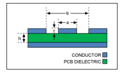
Microstrip line is an ideal choice for high frequency signal transmission on PCB.微帶線是在PCB上傳輸高頻信號的理想選擇。 Unless the connection distance between IC and antenna is very short, please use coaxial cable or transmission line with matching characteristic impedance.除非IC和天線之間的連接距離很短,否則請使用具有匹配特性阻抗的同軸電纜或傳輸線。 On the printed circuit board, it is best to use a microstrip transmission line with the structure shown in the figure below.在印刷電路板上,最好使用具有下圖所示結構的微帶傳輸線。
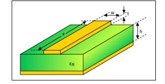
微帶傳輸線包括固定寬度的金屬走線(導體)和正下方(相鄰層)的接地區域。 例如,第1層(頂層金屬)上的走線需要在第2層上有堅實的接地區域。走線的寬度,電介質層的厚度和電介質的類型決定了特性阻抗(通常為50Ω或75Ω)。
當然,除了微帶線以外,還有一條普通的傳輸線是帶狀線,如下圖所示
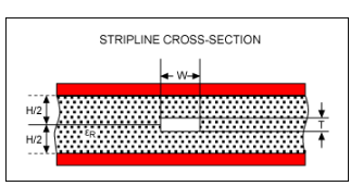
The stripline includes fixed-width traces on the inner layer, and grounding areas above and below it.帶狀線在內層上包括固定寬度的走線,並在其上面和下麵包含接地區域。 The conductor can be located in the middle of the ground area or have a certain offset.導體可以位於接地區域的中間或具有一定的偏移量。 This method is suitable for the inner radio frequency routing.此方法適用於內部射頻路由。
由於帶狀線也適用於RF路由,為什麼老吳說微帶線是PCB上高頻信號傳輸的理想選擇?
無論是微帶線還是帶狀線,兩者在傳輸毫米波頻率方面均具有出色的性能,而不同之處在於製造成本。
Compared with stripline circuits, microstrip circuits have fewer processing steps, and circuit components are easier to place, and therefore easier to manufacture (lower manufacturing costs).與帶狀線電路相比,微帶電路的處理步驟更少,電路元件更易於放置,因此更易於製造(降低製造成本)。 Compared with microstrip lines, strip lines can provide more isolation for adjacent circuit lines and support a denser component layout.與微帶線相比,帶狀線可以為相鄰的電路線提供更多的隔離,並支持更密集的組件佈局。 In addition, stripline circuits are also very suitable for manufacturing multilayer circuit boards, and each layer can be well isolated.另外,帶狀線電路也非常適合於製造多層電路板,並且每一層都可以很好地隔離。
The electrical properties of microstrip and stripline conductors are affected by the dielectric constant of the insulating material and the proximity effect of the ground layer.微帶線和帶狀線導體的電性能受絕緣材料的介電常數和接地層的鄰近效應的影響。 The microstrip line has only one ground plane, while the stripline has two ground planes.微帶線只有一個接地平面,而帶狀線只有兩個接地平面。 For a microstrip line, the effective dielectric constant that affects the impedance of the conductor is the sum of the relative dielectric constant of the insulating material and the air above the circuit (equal to 1).對於微帶線,影響導體阻抗的有效介電常數是絕緣材料和電路上方空氣的相對介電常數之和(等於XNUMX)。 The effective dielectric constant of the strip line is the sum of the relative dielectric constants of the upper and lower substrates of the conductor.帶狀線的有效介電常數是導體的上下基板的相對介電常數的總和。
As with all high-frequency circuits, keeping impedance under control is critical to achieving consistent amplitude and phase response electrical performance.與所有高頻電路一樣,保持阻抗處於受控狀態對於實現一致的幅度和相位響應電性能至關重要。 The impedance of the conductors of the two transmission lines is, among other factors, a function of the width of the conductor, the thickness of the conductor, the thickness of the insulating substrate, and the relative permittivity or dielectric constant of the substrate.除其他因素外,兩條傳輸線的導體的阻抗是導體的寬度,導體的厚度,絕緣基板的厚度以及基板的相對介電常數或介電常數的函數。 For strip lines, it does not matter whether the distance between the center conductor and the two ground planes is equal, or whether the dielectric constants of the insulators above and below the conductor are the same (the same is true for microstrip lines).對於帶狀線,中心導體與兩個接地平面之間的距離是否相等或導體上方和下方的絕緣子的介電常數是否相同(微帶線也是如此)並不重要。
帶狀線有兩個接地層,因此帶狀線的50Ω(或任何給定的阻抗)線比具有微帶線相同阻抗的導體細。 儘管較細的導線支持更大的電路密度,但是較細的導線也需要更嚴格的製造公差,並且整個電路基板的介電常數必須非常一致。 微帶線的單端(不平衡)傳輸線的介電損耗(由基板的損耗因子定義)小於帶狀線的介電損耗。 這是因為微帶線的某些場線在空中,並且可以忽略耗散因數。
Of course, the performance of these two transmission lines is actually almost the same as the performance of the carrier used in their manufacture-the insulating substrate.當然,這兩條傳輸線的性能實際上與在其製造中使用的載體(絕緣基板)的性能幾乎相同。 Just as the PCB materials used, such as FR-4, can reduce costs, but at the same time limit its performance.正如所用的PCB材料(例如FR-XNUMX)可以降低成本,但同時也限制了其性能。 According to different microstrip lines and strip line applications, choosing the most suitable material will better play the role of these two transmission lines.根據微帶線和帶狀線的不同應用,選擇最合適的材料將更好地發揮這兩條傳輸線的作用。 advantage.優點。
As with many engineering decisions, the choice of microstrip or stripline will be weighed.與許多工程決策一樣,將對微帶或帶狀線的選擇進行權衡。 For example, stripline circuits have a high circuit density.例如,帶狀線電路具有高電路密度。 Therefore, under the same frequency conditions, they require more material layers, more processing time and expense, and more attention to detail processing than microstrip circuits.因此,在相同的頻率條件下,與微帶電路相比,它們需要更多的材料層,更多的處理時間和更多的費用以及對細節處理的關注。
Compared with common microstrip lines and strip lines, there is another type of radio frequency transmission line that is grounded coplanar waveguide, which provides better isolation between adjacent radio frequency lines and other signal lines.與普通的微帶線和帶狀線相比,還有另一種類型的射頻傳輸線是接地的共面波導,可以在相鄰的射頻線和其他信號線之間提供更好的隔離。 This medium includes the middle conductor and the grounding area on both sides and below as shown below:該介質包括中間導體以及兩側和下方的接地區域,如下所示:
建議通過“柵欄”將其安裝在接地共面波導的兩側,如下圖所示。 此頂視圖提供了在中間導體每一側的頂部金屬接地區域中安裝一排接地通孔的示例。 頂層產生的環路電流短路到下面的接地層。
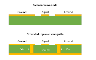
Compared with the microstrip line, the grounded coplanar waveguide not only has a ground plane on the bottom surface of the medium, but also has ground planes on both sides of the signal transmission line on the top of the medium, so it has a larger ground area.與微帶線相比,接地共面波導不僅在介質的底面上有一個接地平面,而且在介質頂部的信號傳輸線的兩側都有一個接地面,因此接地面積更大。區。 The coplanar waveguide achieves the stability of electrical performance by using the ground plane to surround the signal line.共面波導通過使用接地平面圍繞信號線來實現電性能的穩定性。
The transmission modes of the microstrip line and the grounded coplanar waveguide circuit are both quasi-transverse electromagnetic modes (quasi-TEM).微帶線和接地的共面波導電路的傳輸模式均為準橫向電磁模式(準TEM)。 Due to the enhanced grounding structure of the grounded coplanar waveguide circuit, its machining is more complicated to a certain extent.由於接地的共面波導電路的增強的接地結構,其加工在一定程度上更加複雜。 Compared with the microstrip line, the grounded coplanar waveguide circuit has the characteristics of low dispersion.與微帶線相比,接地共面波導電路具有色散低的特點。 When the frequency rises to the millimeter wave band, the grounded coplanar waveguide circuit has lower radiation loss than the microstrip line circuit.當頻率上升到毫米波段時,接地的共面波導電路的輻射損耗比微帶線電路低。
Due to the enhanced grounding structure, the grounded coplanar waveguide circuit has a wider effective bandwidth and a larger impedance range than the microstrip circuit.由於增強了接地結構,接地的共面波導電路比微帶電路具有更寬的有效帶寬和更大的阻抗範圍。 However, the microstrip circuit structure is relatively robust, and its simple bottom ground circuit structure is easy to process.然而,微帶電路結構相對堅固,並且其簡單的底部接地電路結構易於加工。 In addition, the performance of the microstrip circuit is not sensitive to circuit processing factors, and its circuit performance is less affected by the difference in conductor/gap etching and the difference in conductor thickness.另外,微帶電路的性能對電路處理因素不敏感,並且其電路性能受導體/間隙蝕刻的差異和導體厚度的差異的影響較小。
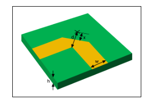
RF電路佈局中的尖銳彎頭是專為傳輸線彎頭補償而設計的。
When the transmission line is required to bend (change the direction) due to wiring constraints, the bending radius used should be at least 3 times the width of the intermediate conductor.當由於接線限製而要求傳輸線彎曲(改變方向)時,使用的彎曲半徑應至少為中間導體寬度的XNUMX倍。 In other words:換一種說法:
彎曲半徑≥3×(線寬)。
這使拐角的特徵阻抗變化最小。
If it is impossible to achieve gradual bending, the transmission line can be bent at right angles (non-curved), as shown in the figure below.如果無法實現逐漸彎曲,則可以將傳輸線彎曲成直角(非彎曲),如下圖所示。 However, this must be compensated to reduce the sudden change in impedance caused by the increase in the local effective line width when passing through the bending point.但是,必須對此進行補償,以減少因通過彎曲點時局部有效線寬的增加而引起的阻抗突變。
我們的其他產品: